SnO - P4/nmm
1. Structure Summary
Last Updated |
2022-12-09 |
Crystal Prototype |
AB |
Crystal System |
Square |
Lattice Constant a (Å) |
3.818 |
Lattice Constant b (Å) |
3.818 |
Space Group |
P4/nmm |
Formation Energy (eV/f.u.) |
-2.5952 |
2. Mechanical Properties (PBE)
2.1 Stiffness Tensors
Cij (N/m) |
xx |
yy |
zz |
xx |
48.140 |
38.957 |
0.000 |
yy |
38.957 |
48.140 |
0.000 |
zz |
0.000 |
0.000 |
38.959 |
2.2 Compliance Tensors
Sij (m/N) |
xx |
yy |
zz |
xx |
0.060189 |
-0.048708 |
0.000000 |
yy |
-0.048708 |
0.060189 |
0.000000 |
zz |
0.000000 |
0.000000 |
0.025668 |
2.3 Orientation-Dependent Mechanical Properties
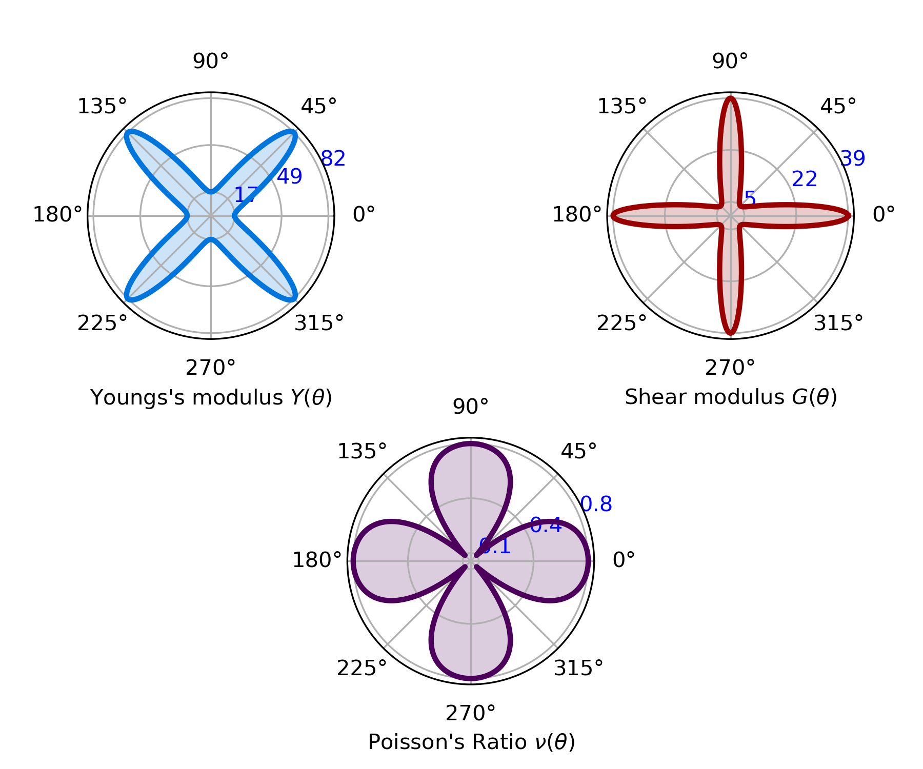
2.4 Anisotropic Mechanical Properties Of 2D Singlecrystal
Mechanical Properties |
Min |
Max |
Anisotropy |
Young’s Modulus (N/m) |
16.614 |
82.252 |
4.951 |
Shear Modulus (N/m) |
4.591 |
38.959 |
8.485 |
Poisson’s Ratio |
0.056 |
0.809 |
14.548 |
2.5 Anisotropic Mechanical Properties Of 2D Polycrystal
Mechanical Properties |
Min |
Max |
Anisotropy |
Young’s Modulus (N/m) |
43.549 |
43.548 |
4.951 |
Shear Modulus (N/m) |
21.775 |
8.215 |
8.485 |
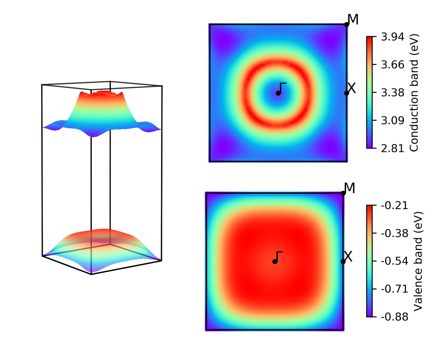
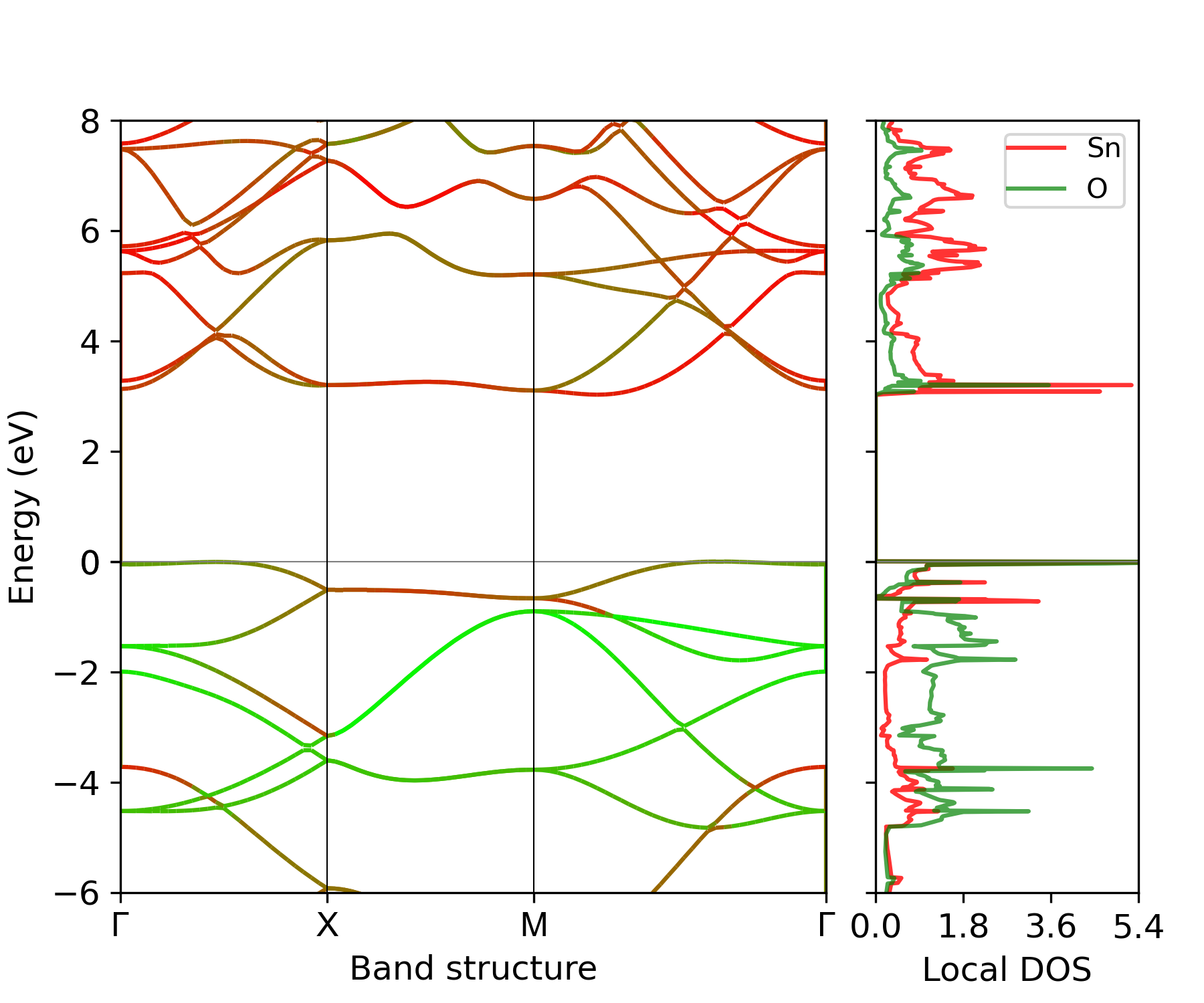
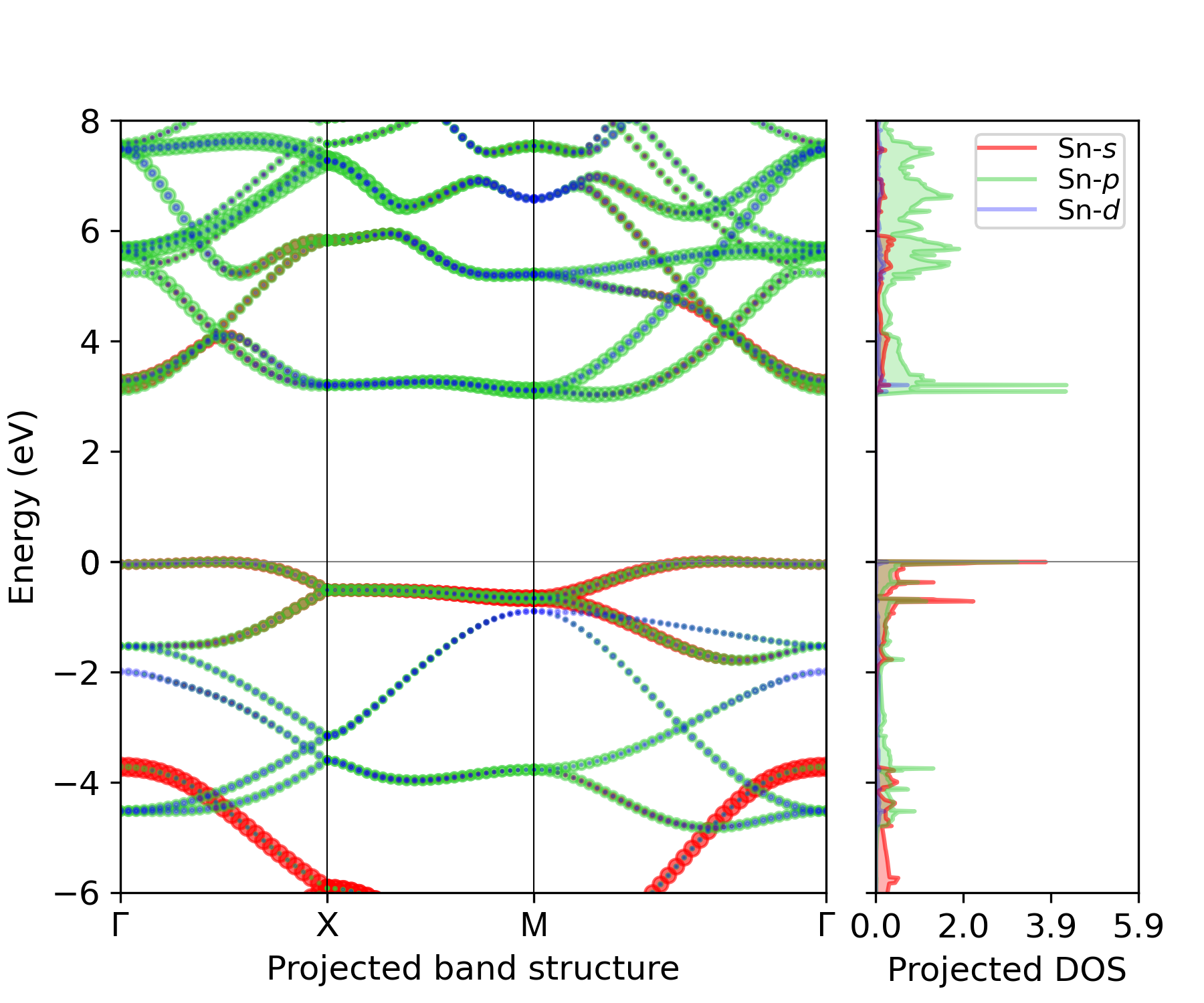
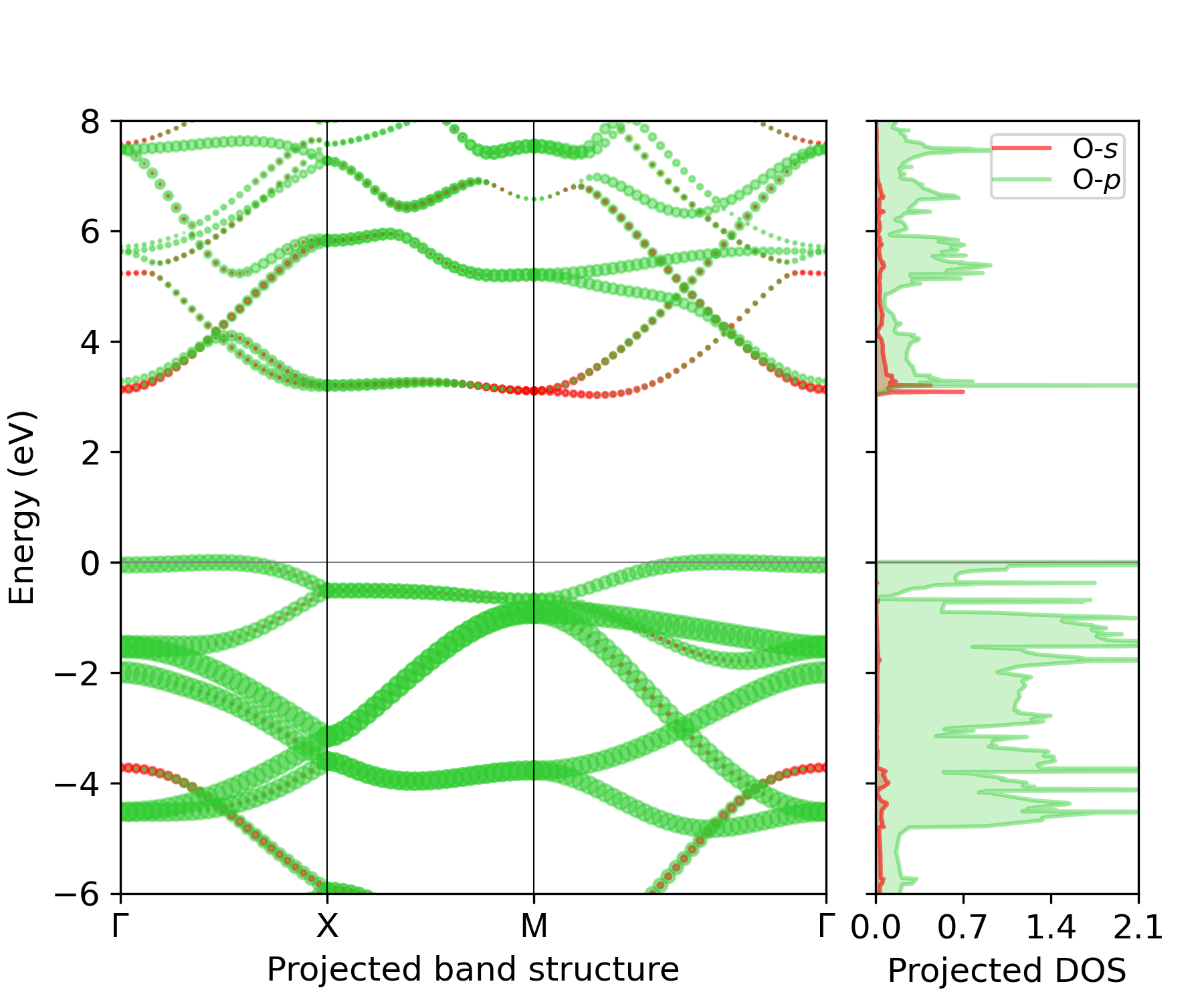
3. Fundmental Electronic Properties
Band Character |
Indirect |
Band Gap (PBE, eV) |
3.0241 |
Band Gap (HSE, eV) |
3.9502 |
Ionization Energy (HSE, eV) |
-5.997 |
Electron Affinity (HSE, eV) |
-2.047 |
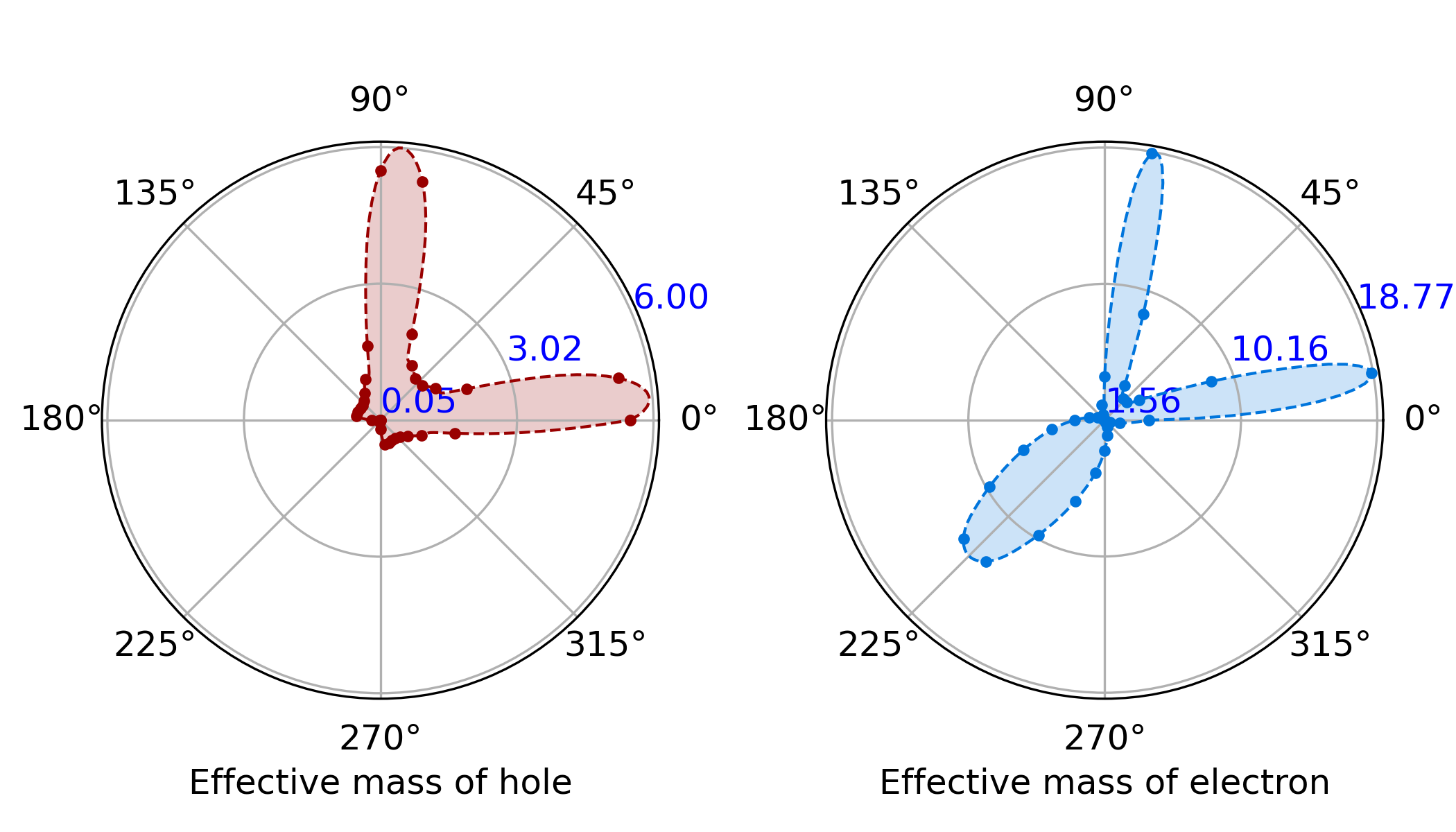
Effective Mass of Electron Max. (m0) |
5.998 |
Effective Mass of Electron Min. (m0) |
0.048 |
Effective Mass of Hole Max. (m0) |
18.770 |
Effective Mass of Hole Min. (m0) |
1.556 |
Location of Valence Band Maximum |
[0.176471, 0.176471] |
Location of Conduction Band Minimum |
[0.382353, 0.382353] |
3.1 Global Band Structure (PBE)
3.2 Band Structure and Density of States (PBE)
3.4 Orientation-Dependent effective Masses (PBE)
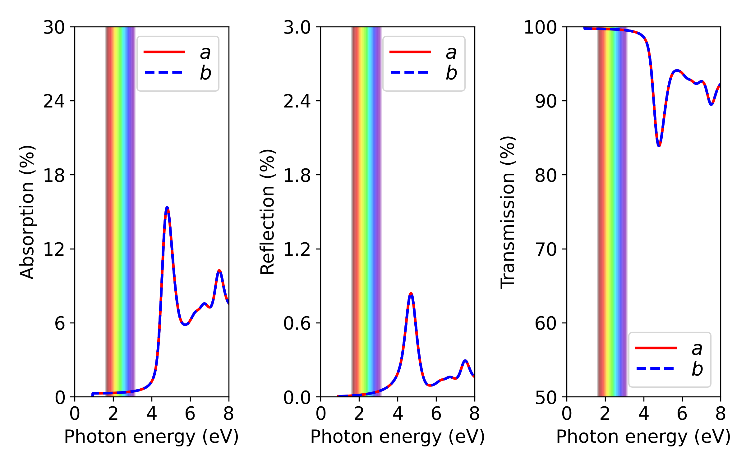
4. Optical Spectrums (HSE)
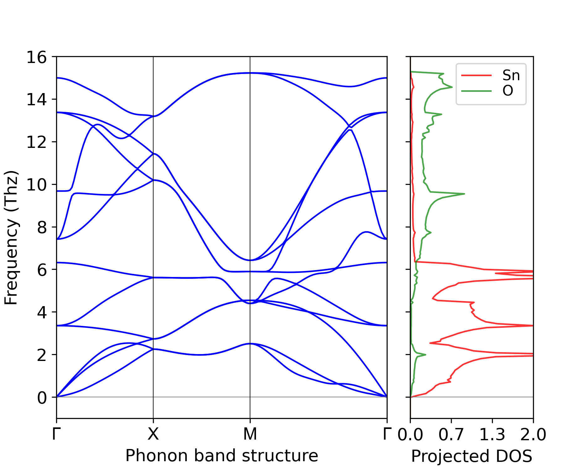
5. Phonon Spectrum and Density of States (PBE)
References
Note
For more details of this database, please refer to the following reference.
[1] V. Wang, G. Tang, Y.-C. Liu, R.-T. Wang, H. Mizuseki, Y. Kawazeo, J. Nara, W.-T. Geng, High-Throughput Computational Screening of Two-Dimensional Semiconductors, Journal of Physical Chemistry Letters 13, 11581 (2022).
License
The contents of this web page are licensed under a Creative Commons 4.0 Attribution International License unless another license is specially mentioned in each web page.